PCB Milling Adventures
After working on the trianglebot’s hardware and software for the last few weeks I thought that I’d take a break and work on some other miscellaneous electronics related to the trianglebot. I need to hook the encoders (5v) up to the beaglebone encoder inputs (3.3v), and I have always wanted to try milling PCBs on my CNC, so here we go! A few weeks ago I ordered some single-sided copper-clad FR4 with intentions of doing this, so I conveniently had all of the materials on hand.
Setup
The longest and most important step of my adventure in PCB milling was the setup. It’s important when milling PCBs to have your copper-clad board very flat so you can have a consistent cutting depth when doing isolation routing. My CNC is pretty flat and square but there are still small variations that cause imperfections when milling PCBs so I decided to take the time to do it the right way from the start and not cut any corners. From my research there are two main ways to get a consistent depth of cut when milling PCBs: surfacing an area and then mounting your copper-clad to it, and using the software “bed leveling” (compensation) tools built into most 3D printer firmware. For me, usually the software fix is the easiest so I decided that I would try and use the bed leveling feature before I went and surfaced my milling area.My CNC which is an MPCNC Primo uses an SKR Pro as the control board that comes by default with custom built Marlin firmware configured for this specific CNC. Unfortunately this default firmware does not come with the bed leveling feature enabled so I had to add additional configuration to the firmware to enable bed leveling, probe offsets, and other minor features. To configure the firmware, V1 Engineering who makes the MPCNC, releases the source code for their custom firmware configuration so I could easily just add on to their configuration rather than starting from scratch.The Marlin firmware uses the PlatformIO build system, which I’m familiar with, and configuring it is as simple as editing some defines in a configuration header, so overall the experience was pretty straightforward. I enabled the bilinear bed leveling feature, set the probe offsets to be all zero (probe is same as the nozzle/bit tip), and recompiling the firmware was super slick thanks to PlatformIO. Flashing firmware to the SKR Pro is also quite easy, you just put the firmware binary on an SD card and insert it into the SKR Pro. Unfortunately for me the control board for my CNC is tucked into a wooden compartment underneath the table so I had to disassemble that to flash the SKR Pro. Getting started with bed leveling was a bit annoying at first, but eventually once I figured out how to use the bed leveling G29 command I made a macro for it in CNCjs. After all this setup my workflow is pretty simple:
- Load isolation routing G-Code into the CNCjs interface
- Run my macro for automatically leveling the bed using a grid the size of the PCB (luckily my leveling probe is a simple conductive touch switch and PCBs are obviously conductive so I can use the tip of the bed and the PCB to easily and conveniently serve as a leveling probe.)
- Run isolation routing program!
The PCB
My goal was to eventually make a PCB that could level shift the signals for all three encoders on the triangle bot but for a start, I just wanted to design a small PCB that would level shift one encoder to test the capabilities of PCB milling on my CNC. I designed the PCB in KiCAD and to convert it to G-Code I first exported it as the Gerber files commonly accepted by PCB manufacturers. The next step and getting the PCB ready for manufacturing was to convert the Gerbers to toolpaths for the CNC. To do this I used a convenient piece of software that I found called pcb2gcode which comes with an easy-to-use GUI. The few changes I had to make to the default pcb2gcode configuration was to change the size of the milling bit I would use to do the cutout and I also enabled the Voronoi regions feature which maximizes the width of tracks and reduces the amount of milling but doesn’t preserve the precise shape of footprints, which was just fine for this PCB. Otherwise the default settings worked perfectly fine for me including the 0.05 mm depth of cut when isolation routing. After this configuration pcb2gcode produces 3 G-Code programs: one for isolation routing, one for drilling, and one for the final cutout. I have my copper clad board attached to its milling surface using blue tape and super glue so I don’t need to use any tabs when doing the cutout, but pcb2gcode does have this feature. I always think it’s a good idea to throw the G-Code into a G-Code simulator like ncviewer just to make sure that everything looks okay before I run it on the actual machine. Everything looked fine on the first try so I went ahead and got the machine all set up for actually milling the PCB.
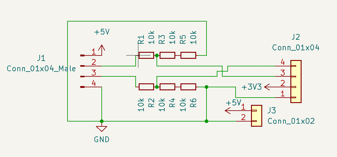
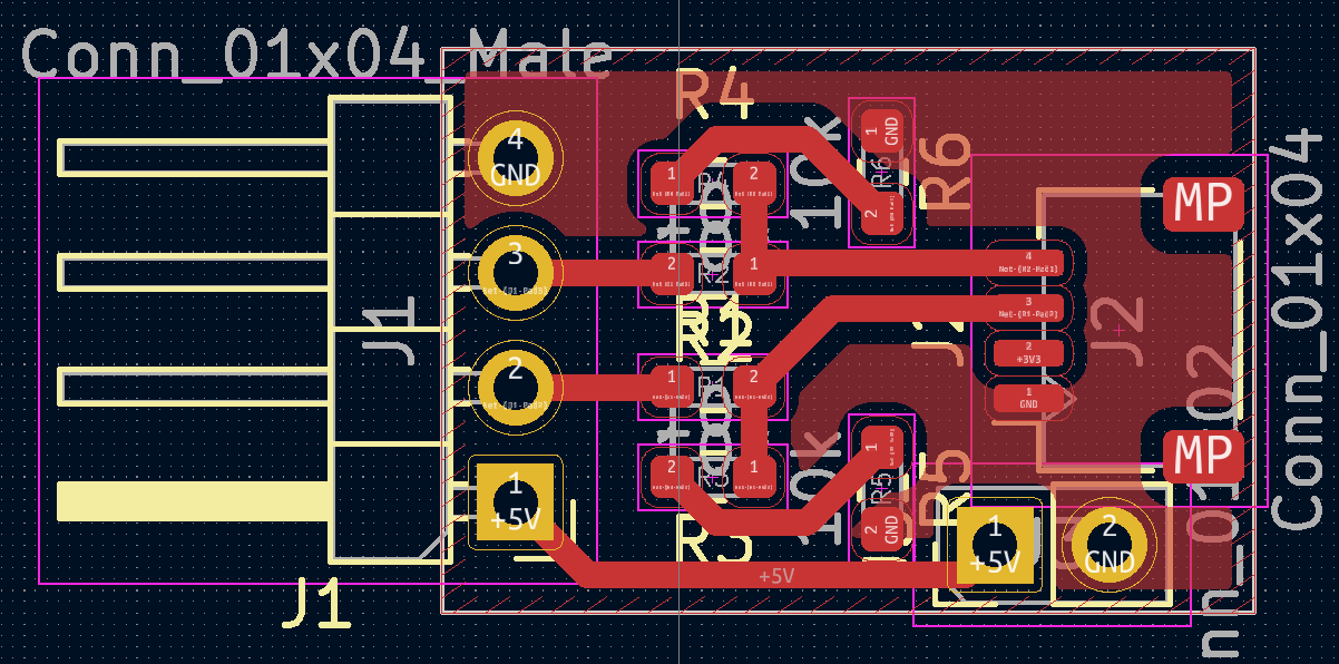
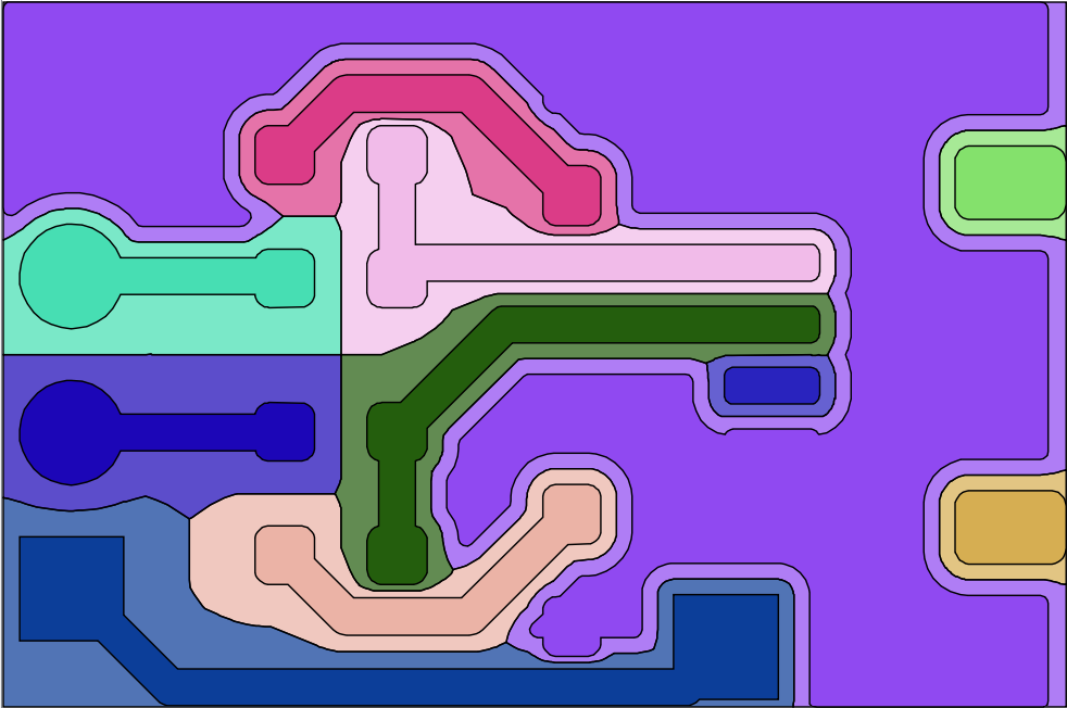
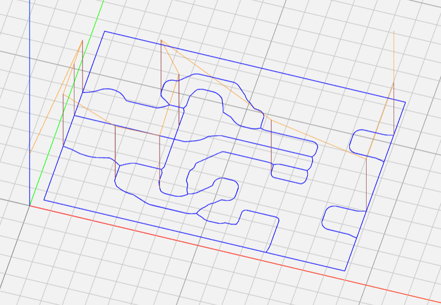
Milling!
Since I had already got bed leveling setup on the CNC and created a macro to automate that process, getting the machine set up for PCB milling was pretty quick. As I mentioned earlier I attached my copper-clad board to a piece of half inch MDF by using the classic trick of attaching blue tape to both surfaces and super gluing them together, this works super well and I highly recommend it for small precision work. The bit that I used for isolation routing wasn’t anything too fancy, just a 60° v-tip mill from a cheap set of bits found online. Once I’d ran the bed leveling procedure I went ahead and ran the g code for isolation routing on my PCB, I was quite surprised at the quality of the results, my router which is a Rotozip RZ1 has a not-insignificant amount of runout so I was surprised to see how well it performed when milling tiny precise tracks.
The next step was to drill the through holes in the PCB, to do this I planned on using the same bit that I was going to use for the cutout, which in retrospect was probably not the best idea. The bit that I was going to use for this was a 1mm two flute straight edge cutter that came in the same set of bits as the V bit I used for isolation routing. Unfortunately due to my router’s run out and the low quality bit, the holes ended up being more like 1.5mm Which is less than optimal for mounting pin headers but was still workable. After I had drilled the holes I immediately ran the cutout program which used the same bit and the results were satisfactory.
Assembly
I’ve had experience assembling PCBs before, and this was no different aside from the lack of a stencil or solder mask. I first applied solder paste to the pads where I was to attach the components using a fine-tipped syringe and then placed the components with tweezers. After the components were placed (the tiny JST SH connector commonly referred to as a “Qwiic” connector thanks to SparkFun, and the 6 tiny 0603 resistors), I put the completed assembly in my reflow oven which is an entry-level Puhui T-962 model, and ran the standard reflow curve for the type of solder paste I used (Sn63 Pb37). After reflowing my PCB was pretty much done!
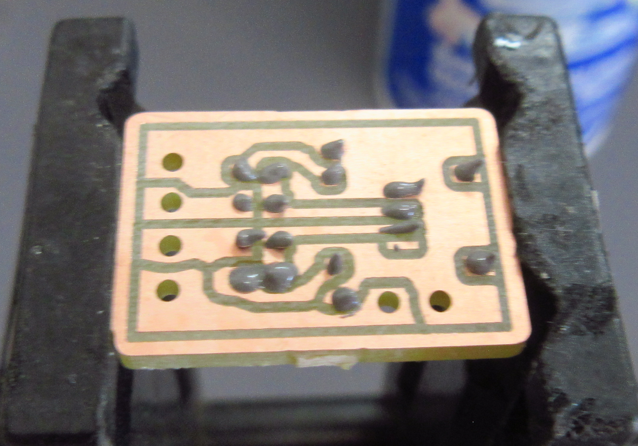
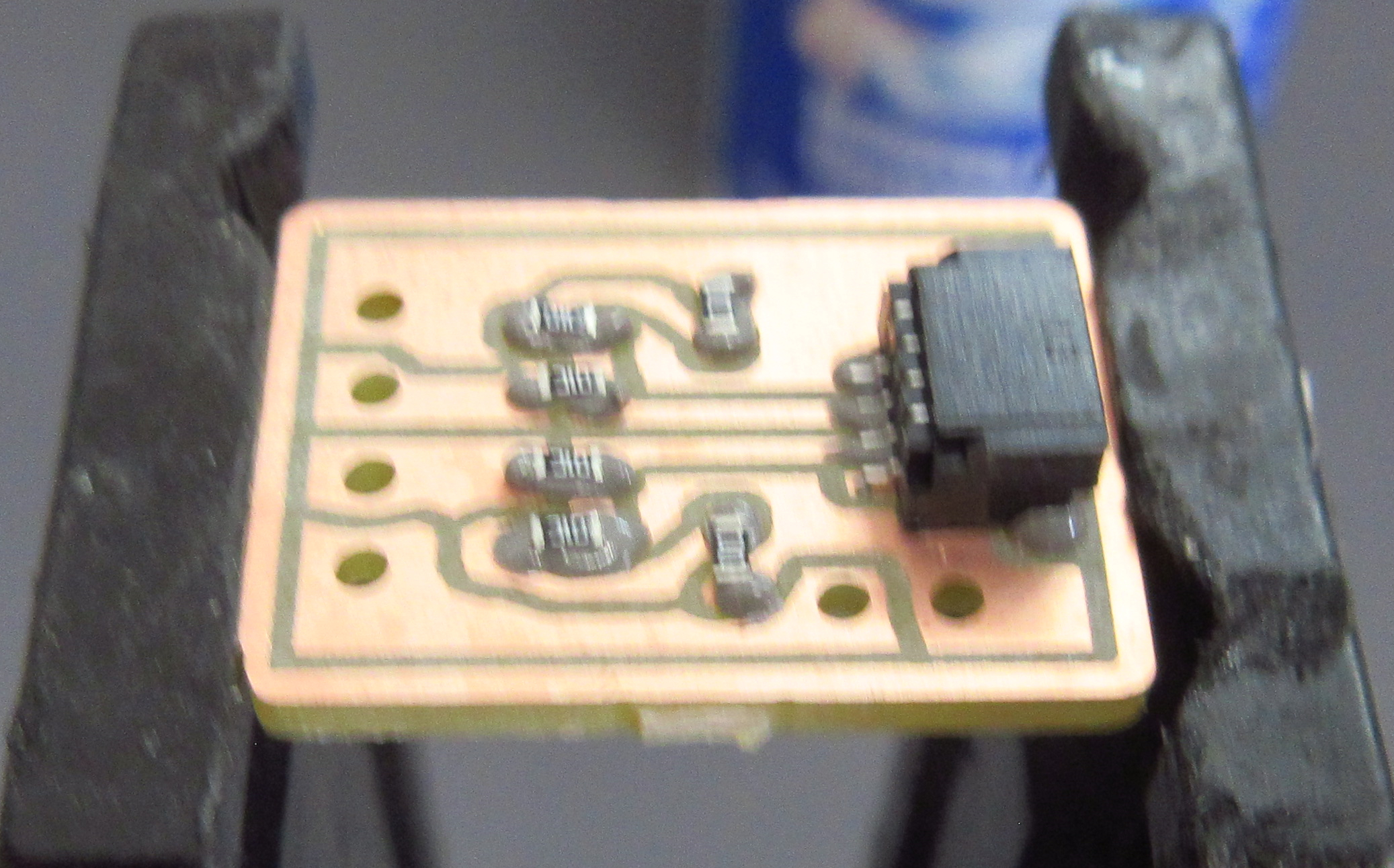
I did some quick testing to make sure that there weren’t any shorts or anything and it properly reduced the signals to 3.3v without major distortion, and I promise I’ll show the full setup when I get around to making another blog post for the trianglebot’s software.
Thanks for reading!